9.2.7
Electron microscopes
The
transmission electron microscope was invented in 1931 by Max Knoll and Ernst
Ruska who realised that electron waves in an 'electron microscope’
would produce much higher resolving power than light waves in an optical
microscope.
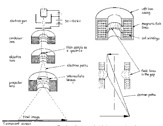
The
above diagram on the left shows an outline of the transmission electron
microscope in which the beam of electrons passes through the sample to form an
image on a fluorescent screen. The electrons are produced by thermionic emission
from a filament wire and are accelerated through a p.d. of between 50 to 100 kV.
The system of magnetic lenses is capable of 106 times magnification. The de
Broglie wavelength of the electrons is sufficiently small to resolve details to
less than 0.5 nm.
The
principle of the magnetic lens is shown in the above diagram on the right.
Electrons passing near the gap in the soft iron shield are deflected towards the
axis of the microscope; electrons passing through the centre are undeflected.
Hence the magnetic lens can be compared with an optical convex lens which
deflects light rays passing near the edge towards the centre and allows light
rays straight through at the centre.
The
condenser lens deflects the electrons into a wide parallel beam incident
uniformly on the sample. The objective lens then forms an image of the sample.
The projector lens then casts a second image onto the fluorescent screen.
The
amount of detail in the image is determined by the resolving power, which
increases as the wavelength of the electrons decreases. Since the wavelength
becomes smaller at higher electron speeds, raising the anode potential in the
microscope gives a more detailed image. However, in practice, the amount of
detail possible is limited by two main factors:
· Lens
aberrations
because the
lenses are unable to focus electrons from each point on the sample to a point on
the screen since some electrons are moving slightly faster than others;
·
sample thickness, because the
passage of electrons through the sample causes a slight loss of speed of the
electrons which means that their wavelength is slightly increased, thus reducing
the detail of the image.
Additional
notes on TEM
1.
The whole arrangement is contained in a high vacuum to prevent electron
collisions with air molecules which would degrade the image.
2.
The specimen must be very thin to minimise lens aberration – typically
50 nm – to minimise the spread of emerging electron energies which would
decrease resolution.
3.
The maximum resolution of optical microscopes is about 2 x 10⁻⁷ m.
Electron microscopes operating at 100kV have a de Broglie wavelength of about
105 times smaller than blue light meaning a maximum resolution of
2 x 10-12 m. In
practice the best achievable resolution is 2 x 10⁻¹⁰ m.
The
scanning tunnelling microscope
The
scanning tunnelling microscope (STM), invented in 1981, gives images of
individual rows of atoms. The STM is based on a fine-tipped probe that scans
across a small area of a surface. The probe's scanning movement is controlled to
within 1 picometre by piezoelectric transducers. The probe is at a small
constant potential, with the tip held at a fixed height of no more than 1 nm
above the surface. At this height, electrons 'tunnel' across the gap and the
current is used to control the vertical movement of the probe to keep the gap
width constant. Hence, if the probe tip moves near a raised atom, the tunnelling
current increases and this is used to move the probe vertically up to keep the
gap width constant. The vertical resolution is of the order of 1 pm, much
smaller than the size of the smallest atom.
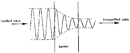
The
principle of tunnelling is based on the wave nature of particles. Light can be
seen through a thin metal film because the amplitude of the light waves is not
reduced to zero by the passage of the light in the film. In the same way, the
amplitude of matter waves in a barrier does not become zero if the barrier is
sufficiently narrow. This process is referred to as 'tunnelling'.
The
'de Broglie wavelength' of an electron depends on its momentum, and equals about
1 nm for electrons in a metal at room temperature. Hence tunnelling is possible
for gaps of the order of 1 nm or so and the tunnelling current is sensitive to
changes of the gap width as little as 1 pm.
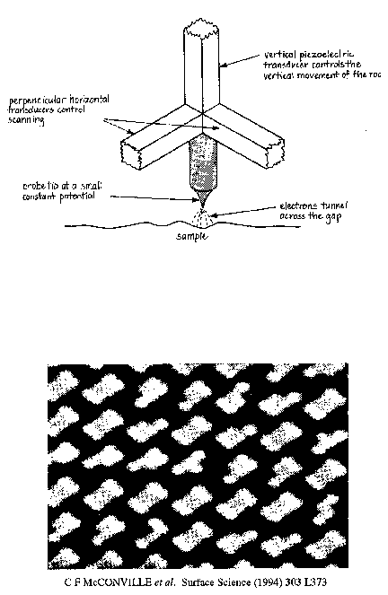
The
above STM image is 10.5 x 7.1 nm. It shows the surface of a semiconductor indium
antimonide (InSb). It shows pairs of Sb atoms arranged in groups of three in a
brick wall type structure. Note that some of the groups are incomplete, each
bright dot indicating a single Sb atom.